| |
Research
Lab Tour
Publications
People
Gallery
Courses
Opportunities
Links
Contact
Home

|
Self-sensing, self-actuating NEMS SPM cantilever at 1 to 5 MHz for parallel, low cost, high speed imaging and lithography.
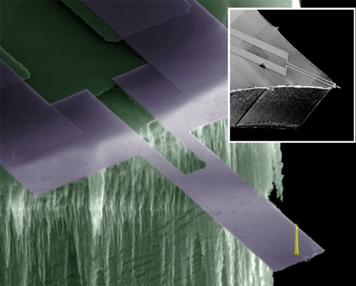
Figure 1. Caltech 1 MHz piezoresistive self-sensing SPM cantilever with tip
Scanning probe microscopy (SPM) is very popular:
- Biologists use atomic force microscopy (AFM) to image cells and proteins.
- Material scientists use magnetic force microscopy (MFM) to map moments of nano-magnets.
- Nano-technologists use dip-pen and tip-enhanced-oxidation lithography to pattern features below 10 nm.
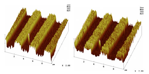
Figure 2. AFM image by commercial system (left) and by Caltech piezoresistive probe
Commercial SPM has excellent imaging quality but limited speed and throughput
- Only one cantilever is operated at a time. It is too expensive in commercial systems to allow two sets of piezo actuator and laser-photodiode sensor. They are also too bulky to let two levers to work in close proximity.
- Newer system could go up to 7 MHz (actual imaging bandwidth is ~ 1/10th). However, there is not yet commercial lever at over 2 MHz. In addition, most people are still operating below bandwidth of 100 kHz.
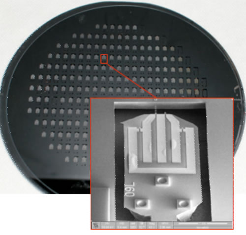
Figure 3. 100mm-wafer scale production of Caltech AFM probe
Caltech NEMS SPM offers high speed and parallel operation
- Parallel operation through cantilever self actuation and sensing
- Self actuation by on chip thermal and piezoelectric drive.
- Self sensing by integrated piezo-resistive sensor.
- Such lever requires only electrical drive and sensing and is cost effective to operate in large array of 1000 or more.
- High frequency NEMS cantilever
- NEMS lever (~ 5 mm ' 300 nm ' 100 nm) has high frequency (1 to 5 MHz) and moderate force constant (100 N/m)
Applications
- Video-frame rate imaging for "fast-shutter" imaging.
- Massive parallel tip-based patterning for semiconductor lithography and photomask repair.
Personnel
Warren Fon, Derrick Chi and Michael Roukes
References
- Mo Li1, H. X. Tang & M. L. Roukes. Ultra-sensitive NEMS-based cantilevers for sensing, scanned probe and very high-frequency applications. Nature Nanotechnology 2, 114 - 120 (2006)
- J L Arlett, J r Maloney, B Gudlewski, M Muluneh, & M L Roukes. Self-sensing Micro- and Nanocantilevers with Attonewton-scale Force Resolution. Nano Letters 2006, Vol 6, No. 5, 1000 1006.

|
