|
|
| Nanowire NEMS | |||
| Research Lab Tour Publications People Gallery Courses Opportunities Links Contact Home
|
Nanoelectromechanical Devices Based Upon Bottom-Up Nanowires
Chemically synthesized (a.k.a., "bottom-up") nanowires are attractive material candidates for nanoelectromechanical resonators because of their ultimately miniaturized sizes and atomically smooth surfaces. We have been interested in both fundamental and engineering aspects of such bottom-up materials and structures. In particular, we have made initial and original efforts in the development of high-performance nanoelectromechanical systems (NEMS) based on various bottom-up nanowires, in close collaborations with leading groups in the fields of materials science and nanowires syntheses. I. Very High Frequency (VHF) Silicon Nanowire (SiNW) NEMS
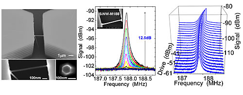
Figure 1. Synopsis demonstration of the VHF SiNW NEMS resonators. (left) SEM images showing typical SiNWs suspended in microtrenches, very straight wires with very well-faceted surfaces and a nice hexagonal cross-section. (middle) Measured resonance responses of a 188MHz SiN NEMS resonator, with very large signal (up to 12.5dB at B=8Tesla in a magnetomotive transduction). (right) Measured resonance responses from the 188MHz device with increasing RF drive levels, clearly showing nonlinear operations at high drive levels. Signals referred to the input of the pre-amplifiers in all the plots. A principal advantage of the suspended SiNW resonators developed in this work is their ease of fabrication and high yield. By pushing the dimensions of the microtrenches downward and simultaneously optimizing the NW growth conditions, we expect that smaller, even molecular-size, suspended SiNWs should be achievable. These will enable scaling fundamental resonance frequencies into the extreme UHF and low microwave range. These SiNW resonators offer significant potential for applications in resonant sensing, quantum electromechanical systems, and high frequency signal processing. We have found that VHF SiNW resonators vibrating at ~200MHz typically have displacement sensitivity of ~5fm/Hz and force sensitivity of 50~250aN/Hz, set by thermomechanical fluctuations. They have ~1nm critical amplitude and intrinsic dynamic range of 90~110dB. These SiNW resonators offer significant potential for applications in resonant sensing, quantum electromechanical systems, and high frequency signal processing. II. Piezoresistive Silicon Nanowire NEMS with On-Chip Electronic Transduction
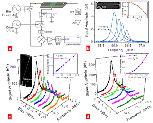
Figure 2. Very high frequency Si nanowire resonators with fully integrated electrostatic actuation and piezoresistive self-detection. (a) Schematic diagram of bias and drive circuitry. (b) Device performance of a 40 nm thick, 96 MHz nanowire resonator with a quality factor Q of ~550. It is 1.8 µm long and has a dc resistance of 80 kΩ. The AC drive is set at Vd,AC= 0.50, 0.63, 0.71, 0.79 V for the curves respectively, with the DC voltage fixed at Vd,DC=0.2 V. The left inset shows the SEM image of the device, and the right inset shows the drive dependence of the resonance frequency. (c) Performance of a 30 nm thick, 75 MHz Si nanowire resonator with Q~700. Its length is 1.8 µm and its dc resistance is 300 kΩ. The curves are taken at different bias voltages with the same drive. The inset shows the SEM image and the linear dependence on bias voltage. (d) Data taken at varied drive with the same bias. Inset shows the quadratic dependence on drive voltage. In this work, we have demonstrated that for very thin Si nanowires, their time-varying strain can be exploited for self-transducing the devices’ resonant motions at the VHF/UHF bands. The strain that is only second-order in doubly clamped structures, enables efficient displacement transducers due to the enhanced piezoresistance effect in these Si nanowires. This self-integrated transduction scheme requires minimum device complexity and operates readily at room temperature and vacuum conditions provided by standard packaging technologies. These devices represent a unique group of nanowire resonators that are as thin as 30 nm, with intrinsically embedded strain transducers and monolithically integrated actuation. Such prototypes should facilitate their direct integration with electronics toward functional systems for various applications. By combining Si nanowire’s piezoresistive self-transducing with off-chip piezoelectric-disk actuation and on-chip electrostatic excitation, we have demonstrated VHF Si nanowire resonators. For devices with widths ranging from 90nm to 30nm, and lengths of 1.8µm to 5µm, the resonators operate at frequencies from 20MHz to 100MHz, with quality factors (Q's) in the range of 5501200, at room temperature and non-stringent vacuum conditions (~mTorr range). The measured Q's do not drop until pressure is raised to ~1Torr and are still appreciable at ~100Torr (e.g., Q~300 for the 30nm thick Si nanowire operating at 75MHz). The down-mixing technique developed for readout of the second-order piezoresistive effects in doubly clamped structures readily provides VHF transduction for devices with progressively shrinking dimensions and high impedances in the range from ~1k to ~1M, without the need for extra patterning or metallization. Our simple and practical demonstration of integrated Si nanowire NEMS should engender many new applications of integrated nanowire resonators and arrays. Personnel References
|
||
| | local users |
|||